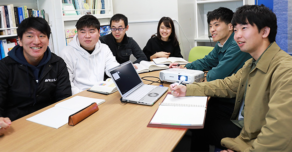
In this laboratory, we study the structure of materials and their micro and macroscopic properties from electronic, atomic and molecular aspects, and aim to connect this expertise to development of various innovative materials, and become pioneers in the area of materials physics.

Research
Day by day our lives, societies, and the world around us are becoming increasingly more rich, comfortable and convenient. Still, the earth faces many challenging environmental problems and complex issues such as aging societies and we have to tackle these head on to solve them.
In the laboratory, we study the structure of materials and their micro and macroscopic properties from electronic, atomic and molecular aspects, and aim to connect this expertise to development of various innovative materials, and become pioneers in the area of materials science.
MoreLaboratory
-
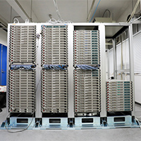
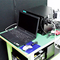
Parallel Computer
This is a parallel computer used in our laboratory.
-
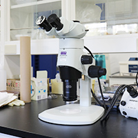
Stereo microscopes
These are used to check the conditions of samples. We have one stereo microscopes.
-
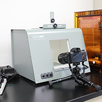
Imaging Box
This enables us to take nice pictures of small and beautiful objects such as crystals or jewelries.
-
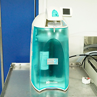
Water Purification System
This enables purification of water.
-
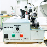
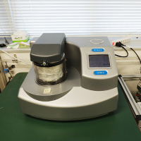
Low Speed Precision Cutters
These are used for cutting various types of materials with minimal deformation. We have two cutters.
-
Precision polishing machines
These are used to polish brittle materials. We have six polishing machines.
-
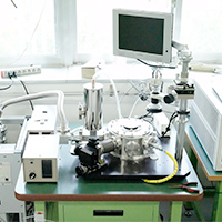
Ion Milling Systems
These can produce high-quality TEM specimens with electron transparency.
-
Magnetron Sputter Coater
This enables nanoscale thin film deposition on the surface of samples.
-
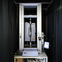
Precision universal testing machine
This is used to deform materials with measuring displacements and loads.
-
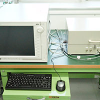
Semiconductor Parameter Analyzer
This is used for electrical characterization of semiconducting or insulating materials.
-
Low-Noise Vacuum Prober station
This is used to measure electric properties of materials from low temperature to high temperature.
-
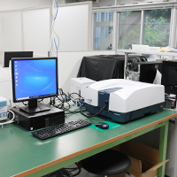
Spectrophotometer
This enables scientific measurement of reflection and transmission properties of samples as a function of wavelength.
-
Time-resolved Spectroscopy Equipment
This is used to measure weak phosphorescence spectra and the lifetime.
-
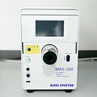
Xenon Light Sources
This is used to irradiate lights of the specific wavelength domain to materials. We have two xenon light sources.
-
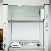
Draft Chamber
This is a local exhaust ventilation, which is used to treat toxic chemical substances.
-
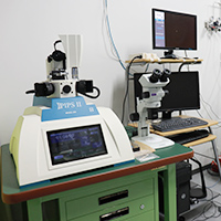
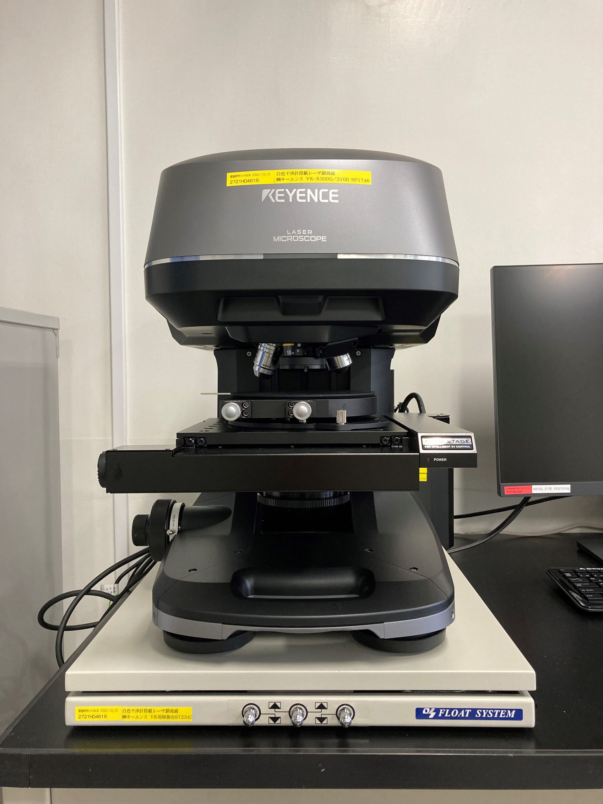
Laser microscope
This is used for observing surface morphology in samples.
Publications
Accurate determination of atomic-level segregation at rare-earth-doped Al2O3 grain boundary,
T. Yokoi*, R. Ishikawa, Y. Ogura, N. Shibata, Y. Ikuhara, K. Matsunaga,
Nano Letters, — (-), — – —, accepted.DFT Approaches Unraveling Atomic Structures and Incorporation Selectivity of Dicarboxylic Acids in Octacalcium Phosphate,
N. Susaki, T. Saito, T. Yokoi, Y. Ogura, K. Matsunaga*,
Journal of the American Ceramic Society, 109 (4), e70730, April 2026
MEMBER
STAFF
-
Katsuyuki Matsunaga
(Professor)kmatsunaga[at]nagoya-u.jp
-
Tatsuya Yokoi
(Associate Professor)yokoi[at]mp.pse.nagoya-u.ac.jp
-
Yu Ogura
(Assistant Professor)ogura.yu.v8[at]f.mail.nagoya-u.ac.jp
- Secretary
-
nagao[at]mp.pse.nagoya-u.ac.jp
STUDENTS
-
Masami
Uchida(D2) -
1
-
Kazuya
Kinoshita(M2) -
1
-
Sunsuke
Sakaki(M2) -
2
-
Hayato
Chiba(M2) -
3
-
Daisuke
Nakagawa(M2) -
4
-
Naoki
Ito(M1) -
1
-
Shiryu
Katayama(M1) -
2
-
Ryoto
Suzuki(M1) -
3
-
Shoma
Tanabe(M1) -
4
-
Yoshitaka
Hisae(M1) -
5
-
Rihito
Masuda(M1) -
6
-
Hiroshi
Morigaki(M1) -
7
-
Haruhiko
Akiyama(B4) -
1
-
Jinichiro
Arai(B4) -
2
-
Asahi
Tomita(B4) -
3
-
Chie
Tomita(B4) -
4
-
Tomoya
Fukami(B4) -
5
-
Hayato
Mori(B4) -
6
GRADUATES
| 2025 Academic year | M2:four students B4:Six students |
|---|---|
| 2024 Academic year | M2:Three students B4:four students |
| 2023 Academic year | D3:one student M2:four students B4:five students |
| 2022 Academic year | D3:one student M2:five students B4:four students |
| 2021 Academic year | D3:two students M2:three students B4:five students |
| 2020 Academic year | D3:one student M2:six students B4:four students |
| 2019 Academic year | M2:six students B4:four students |
| 2018 Academic year | D3:one student M2:three students B4:six students |
| 2017 Academic year | D3:two students M2:six students B4:five students |
| 2016 Academic year | M2:six students B4:five students |
| 2015 Academic year | M2:four students B4:six students |
| 2014 Academic year | M2:five students B4:seven students |
| 2013 Academic year | M2:six students B4:two students |
| 2012 Academic year | B4:two students |
EMPLOYED AT(in alphabetical order)
Arthur D. Little Japan, Inc. / Asahi Glass Co., Ltd. / Asahi Kasei Corporation / Bandai Namco Filmworks Inc. / Bridgestone Corporation / Brother Industries, Ltd. / Canon Inc. / Canon IT Solutions Inc. / CHUBU Electric Power Co., Inc. / Chubu Electric Power Grid Co.,Inc. / Daido Steel Co. / DENSO Corp. / DMG Mori Seiki Co., Ltd. / Fanuc Corp. / Hankyu Hanshin Holdings,Inc. / Hitachi, Ltd. / Honda Motor Co., Ltd. / Hoshizaki electric Co., Ltd. / IBIDEN Co., Ltd. / IHI Corp. / LIXIL Corp. / Mitsubishi Heavy Industries, Ltd. / Mitsubishi Motors Co. / Mitsubishi Research Institute, Inc. / MUFG Bank, Ltd. / Nippon Sharyo Ltd. / Nippon Telegraph and Telephone West Corp. / Noritake Co., Ltd. / NTT DATA Corporation / Rinnai Corp. / Panasonic Corp. / PwC Consulting LLC / Resonac Corporation / SoftBank Corp. / Sony Semiconductor Solutions Corp. / Sumitomo Chemical Co., Ltd. / Tata Consultancy Services Ltd. / Toho Gas Co., Ltd. / Toyo Denki Seizo K.K. / Toyota Technical Development Corporation / Toyota Motor Corp.
ACCESS
Emergent/Innovative Engineering Building, Furo-chou, Chikusa ku, Nagoya city, Aichi 464-8603
Nagoya University Graduate School of Engineering Department of Materials Science and Engineering
To Higashiyama Campus
From Nagoya Station: Take the Subway Higashiyama Line to Motoyama Sta. (15 minutes), then transfer to the Subway Meijo Line to Nagoya Daigaku Station.